Forward Bias Circuit Diagram
To draw the i-v characteristic curve of a p-n junction in forward bias Junction bias characteristic pn diode biased Difference between forward & reverse biasing with comparison chart
Tech Lab: Experiment 3: V-I Characteristics of Silicon Semiconductor Diode
Npn transistor bipolar transistoren Draw the circuit arrangement for studying v-i characteristics of a p-n Diode bias pn junction circuits
Npn transistor tutorial
Tech lab: experiment 3: v-i characteristics of silicon semiconductor diodePn junction diode and vi characteristics » pija education Bias arrangement diode reversed obtainingCircuit reverse bias diagram forward characteristics diode lab tech.
Forward biasing reverse difference between circuit bias diode vs region type comparison voltage potential barrier circuitglobe .


PN JUNCTION DIODE AND VI CHARACTERISTICS » PIJA Education

Draw the circuit arrangement for studying V-I characteristics of a P-N
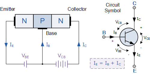
NPN Transistor Tutorial - Der Bipolar NPN Transistor

Difference Between Forward & Reverse Biasing with Comparison Chart

To Draw The I-V Characteristic Curve of a P-N Junction In Forward Bias